Research Highlights:
Electronic transport from first-principle

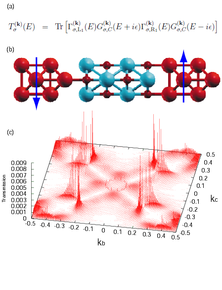
with antiferromagnetic ordering between two Fe electrodes, (c) k-resolved
transmission spectrum across the MgO layer in the structure (b).
As miniaturization of electronic devices has advanced in recent years, the gap between experiments and theories has gradually narrowed. To quantitatively address the quantum electronic transport problem in nano-scale electronic devices, one of most successful methods is the nonequilibrium Green's function (NEGF) method because of the generality of the theoretical framework. We have recently developed an efficient implementation technique of the NEGF method combined with the density functional theory (DFT) using localized pseudo-atomic orbitals (PAOs) for electronic transport calculations of a system connected with two leads under a finite bias voltage [1]. In the implementation, accurate and efficient methods are newly developed especially for evaluation of the density matrix and treatment of boundaries between the scattering region and the leads. Equilibrium and nonequilibrium contributions in the density matrix are evaluated with very high precision by a contour integration with a continued fraction representation of the Fermi-Dirac function [2] and by a simple quadrature on the real axis with a small imaginary part, respectively. The Hartree potential is computed efficiently by a combination of the two dimensional fast Fourier transform (FFT) and a finite difference method, and the charge density near the boundaries is constructed with a careful treatment to avoid the spurious scattering at the boundaries. The efficiency of the implementation is demonstrated by rapid convergence properties of the density matrix. In addition, as an illustration, our method is applied for zigzag graphene nanoribbons, a Fe/MgO/Fe tunneling junction (as shown in Figure), and a LaMnO3/SrMnO3 superlattice, demonstrating its applicability to a wide variety of systems. The research was conducted in collaboration with AIST and NIMS.
- "Efficient implementation of the nonequilibrium Green function method for electronic transport calculations", T. Ozaki, K. Nishio, and H. Kino, Phys. Rev. B 81, 035116 (2010).
- "Continued fraction representation of the Fermi-Dirac function for large-scale electronic structure calculations", T. Ozaki, Phys. Rev. B 75, 035123 (2007).
