

Research Highlights:
Silicene on ZrB2
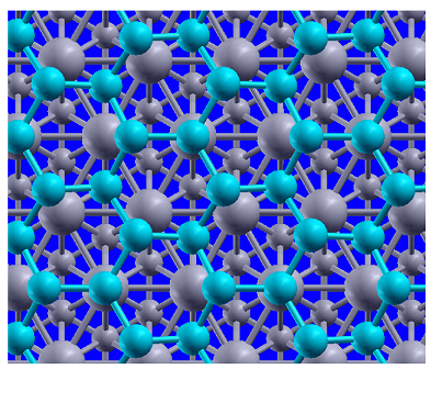
As the Si counterpart of graphene, silicene may be defined as an at least partially sp2-hybridized, an atom-thick, honeycomb layer of Si that possesses pi-electronic bands. Takamura-Yamada group of JAIST recently has succeeded to fabricate two-dimensional, epitaxial silicene through surface segregation on zirconium diboride thin films grown on Si wafers. To support the experimental study, we have performed a series of first-principle calculations for the new material, and compared geometrical structures, the scanning tunneling microscope (STM) image, the chemical shift of the Si2p state, and the band strucure with experimental data in detail [1]. The comparison suggests that a buckled silicene certainly forms on the ZrB2 substrate, and a particular buckling of silicene induced by the epitaxial relationship with the diboride surface leads to a direct pi-electronic bandgap at the Gamma point. These results demonstrate that the buckling and thus the electronic properties of epitaxial silicene are modified by epitaxial strain. The research was conducted in collaboration with Takamura-Yamada and Friedlein groups in JAIST.